

All About Chips & Semiconductors
All About Chips & Semiconductors
A deep dive into the science of today's hottest commodity


Welcome to Space Race, where we explore the impact of breakthroughs in science research on the 21st century. Subscribe for breakdowns of the scientific breakthroughs that will shape the future.
In today’s newsletter we discuss chips and semiconductors. We’ll understand the unique properties of semiconductors and why they are critical to current and future technology. We’ll also demystify the complicated process of making chips from scratch, explore the state of the art in chip manufacture, and see why the global stakes have become so big around these tiny devices.
One of the most notable trends of the post-COVID world is degree of urgency with which many are now talking about “chips” and “semiconductors”. Long the preserve of scientists and engineers toiling away in out of sight labs and fabs, these technologies are now front and centre in a looming global scientific competition. The US recently committed a mammoth $52 billion to its recent CHIPS act, China is pouring immense effort into chip production, and even the Indians and Europeans are jumping into the ring. But what exactly are the microscopic chips and semiconductors that all these global powers are throwing billions behind, and why do they matter so much?
What are Semiconductors
Virtually all the billions of chips that power all our electronics rest on the shoulders of the humble semiconductor, so let’s start there.
One of the fundamental distinctions we can draw when classifying materials in nature is whether they conduct electricity or not. For example, metals like copper are very good conductors of electricity. To see why this is, remember that all materials are made of atoms. Atoms in turn are made up of a small central nucleus of protons and neutrons surrounded by a cloud of negatively charged electrons. What makes metals good conductors is the fact that their electrons are not tightly bound to the atoms but are actually free to move around. These are called delocalised electrons and their motion is what allows electrical current to flow. In addition to metals, some nonmetals like graphene (a simpler version of the graphite in pencil lead) also conduct electricity, because their atomic structure allows for the existence of conduction electrons. By contrast, insulators are materials which do not allow electrical current to flow since there are no free electrons. Glass, plastic, and air are common examples of insulators.
As the name implies, semiconductors fall somewhere in between on this spectrum. Under normal circumstances, semiconductors tend to be insulators as the electrons are tightly bound to their atoms. Unlike pure insulators however, these electrons can be excited into breaking away from their atoms and becoming conduction electrons if enough energy is supplied, for example by heating up the semiconductor. This is why the electrical resistance of a semiconductor (a measure of how much it resists the creation of electrical currents) goes down when it heats up.
Unlike pure insulators or pure conductors, semiconductors can be manipulated by changing their conductivity, and this degree of control is the key behind their foundational role in modern electronics. Common examples of semiconductors include chemical elements such as gallium and compounds such as gallium arsenide. However, the most important semiconductor by far is silicon, used in 95% of all semiconductor devices today.
Doping
Most electronic devices that use semiconductors can’t rely on changing temperatures to control conductivity — you can’t expect your laptop/phone to only work on hot days! Instead, we use a process called doping to allow us to manipulate the conductivity.
Doping refers to inserting impurities within the silicon to improve its conductivity at room temperature. To see how this works, we need to understand how the atoms in silicon are arranged.
A silicon atom has 14 positively charged protons in its nucleus, which means it has 14 negatively charged electrons (to balance out charges). Because of quantum mechanics, these electrons can only exist at certain well defined levels called energy levels or shells, with the lowest energy electrons closest to the nucleus. For conduction, the electrons in the outer most shell are the most important since those are the electrons that can become delocalised easiest. These outer electrons are known as valence electrons.
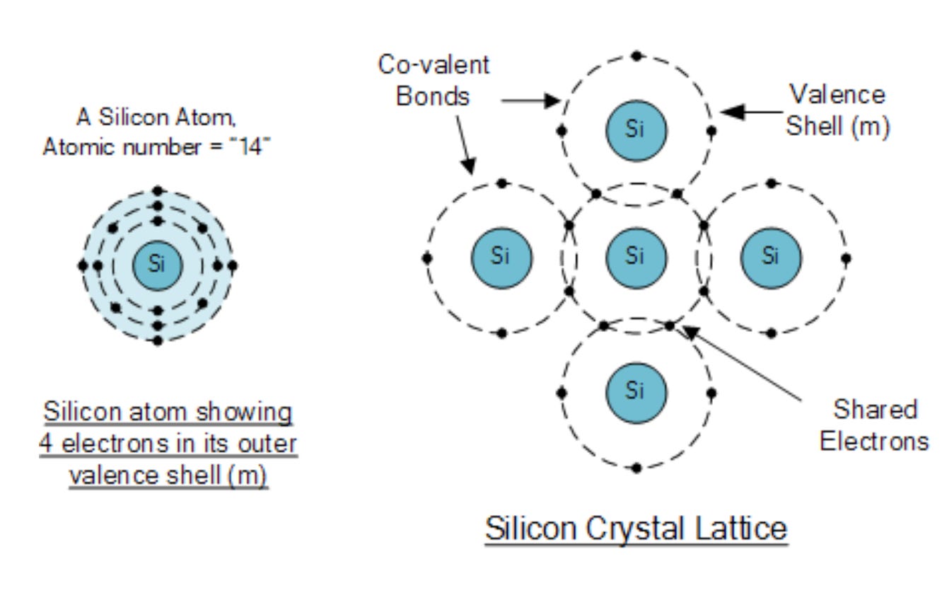
Each silicon atom has 4 valence electrons, and each valence electron forms a pair with a valence electron from a neighbouring silicon atom. This is called a covalent bond and is what holds the atoms together. However in this configuration, there are no electrons available to move around unless we heat the silicon and break them free.
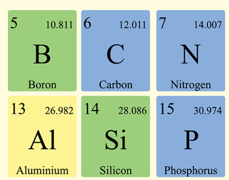
This is where doping comes in. In order to break this stable arrangement, we artificially insert some impurities which will allow electron motion. Common examples of silicon dopants are boron and phosphorus. These are ideal because they are right next to silicon on the periodic table of elements, which means they have similar chemical properties/atomic structure and so will easily embed in the silicon lattice.
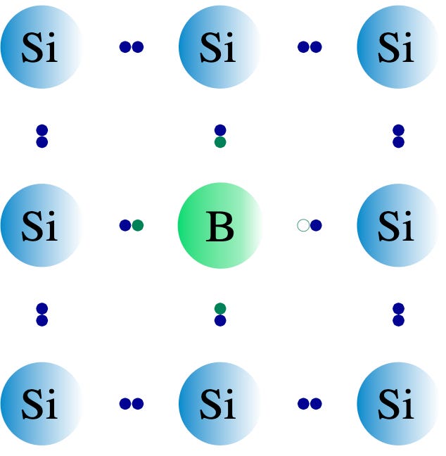
The reason why doping works is because while silicon has 4 outer electrons, boron has 3 while phosphorus has 5. Suppose you replace a silicon atom in the lattice with a phosphorus atom, which slots in nicely because it’s chemically similar. Four of the phosphorus’ outer electrons will bond to its neighbouring silicon atoms, but one will be unbonded and free to move around — electrical current can now flow! Because this doping has added an extra electron, which has a negative charge, we call this n-type doping.

The idea with boron is the same. Instead of adding an extra electron however, boron has only 3 outer electrons so it actually creates a space for another unpaired electron to move into. In the picture below, if an electron moves left to fill the empty space in the boron atom, the empty space effectively moves to the right in the opposite direction. Because of this, by convention we say that the empty space, or “hole” behaves like a positive charge carrier moving opposite to the direction of the negative electron, and these positive holes are what carry electrical current in this system. That’s why this is called p-type doping.
Understanding How Transistors Work
Now we have the tools to understand one of the most important pillars of modern electronics: the transistor, of which there are literally billions in virtually all common devices like phones and laptops. What makes transistors so important is how they use the properties of semiconductors to act as switches and amplifiers that can be engineered to minuscule length scales.
To see how all this is possible, let’s use the example of the MOSFET — short for metal-oxide-semiconductor field effect transistor — which is by far the most common type of transistor in digital circuits today. The picture below shows the basic structure.

A MOSFET is made up of a main body of p-type silicon, with two layers of n-type silicon placed on top which are known as the source and drain. The source and drain are electrically connected to other components in the circuit. Above these three, there is a layer of silicon oxide, which is an insulator to protect the system from outside electrical currents.
In its normal state, the p-type body has extra holes which the extra electrons in the n-type layers quickly fill. Once these holes are filled, no electrons can move and no current can flow between source and drain. The MOSFET is in its “off” state.
However, if we apply a positive voltage at the gate terminal, this exerts an attractive force on the extra electrons in the source and drain. This is because opposite charges attract and the electrons in the source and drain are attracted to the positive charge in the gate. However due to the silicon oxide protection, they cannot actually travel up to the gate and are instead forced through the p-type body. With a strong enough voltage, the electrons are forced all the way from source to drain and the electrical path is now complete. Current can now flow and the MOSFET is in its on state and we have now created a voltage controlled switch.
The amazing thing about MOSFETs and transistors is that they allow us to create electrical switches (and amplifiers!) without any moving parts. Just by controlling the voltage at the gate, you can flip the MOSFET on and off. The lack of mechanical parts is a huge reason why MOSFETs and other semiconductor based electronics can be made at minuscule length scales, touching the nanometer level. This small size is crucial, because it allows packing of literally billions of transistors into dense electrical circuits, which are known as integrated circuits or more commonly as chips. Apple’s new M1 Ultra chip, which has a mammoth 114 billion transistors, is just one example of this.

How Are Chips Made?
Semiconductors make it possible to make very small electronic components, but it takes a high degree of expertise to fabricate chips with billions of transistors on them. Chip manufacture requires dedicated fabrication plants — aka fabs — with very specialised equipment and very highly skilled human labour.
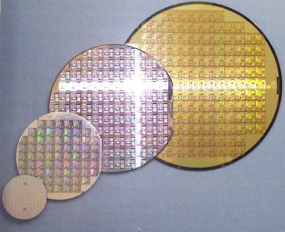
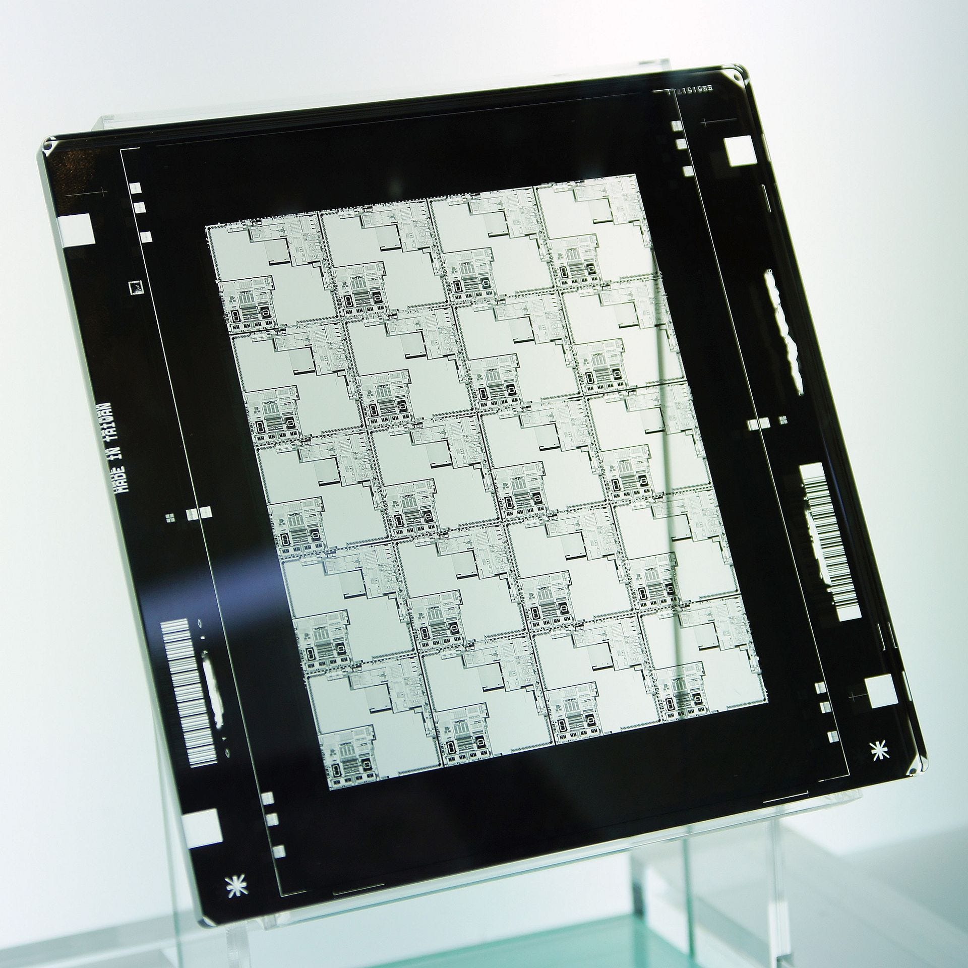
Virtually all chip components are made by building up layers of patterns on a silicon substrate so the chip fabrication process must begin with a very high purity silicon wafer. 99.999999999% pure to be precise, i.e. one impurity per every 100,000,000,000 silicon atoms.
Fortunately, silicon is very abundant — for example it is commonly found in sand in the form of silica or silicon dioxide. By heating the silica with carbon, we can extract silicon. This extracted silicon is then purified to the required level using specialised methods like the Czochralski Process, which creates high purity silicon crystals. Thin wafers are then cut from these crystals, ready for chip production.
For production it is vital that the silicon be protected from contaminants like dust. As a result, chip fabrication must take place in extremely sterile conditions. For example, the air in Intel’s fabs is filtered so that it has 1,000 times fewer airborne particles than a hospital operating room. All objects entering the facility must be thoroughly cleaned and all human skin and hair has to be covered by specialised protective suits, glasses, gloves, and boots.
Once the wafers are ready, the first step is deposition. This is where thin films of conductors, insulators, or other semiconductors are deposited on top of the silicon wafer, with the exact composition depending on the design of the device. A layer of protective silicon oxide is also deposited on top of the wafer.
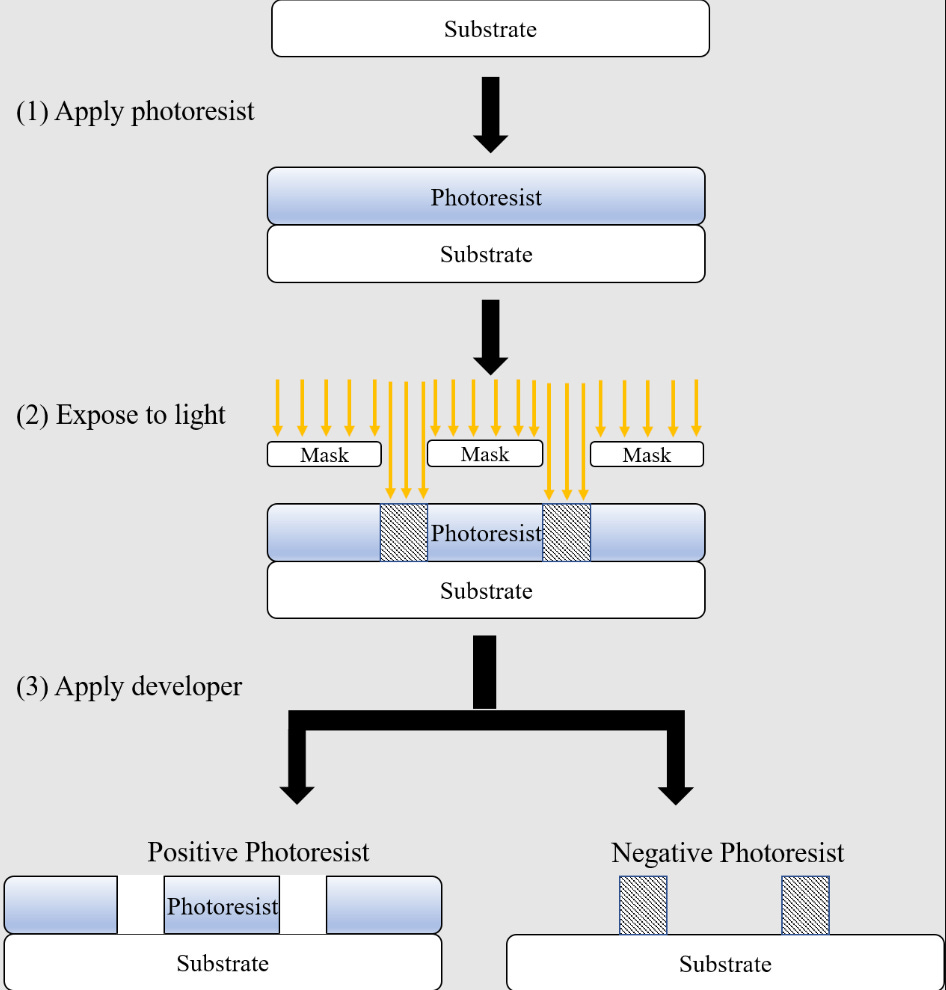
The next step is called lithography, where we “print” the chip design onto the substrate using light. To do this, first a photomask is made, which is an opaque plate patterned to let light through in the pattern corresponding to the chip design.
Once the photomask is ready, the silicon substrate is coated with a light-sensitive material called photoresist. The photomask is placed over this and when unmasked regions of the photoresist are exposed to light, they will react. In the case of positive photoresist, the unmasked regions will become weaker, while negative photoresist makes the unmasked regions stronger. After this, a special chemical called a developer dissolves away the weak regions of the photoresist, leaving the chip pattern engraved in the photoresist on top of the substrate.
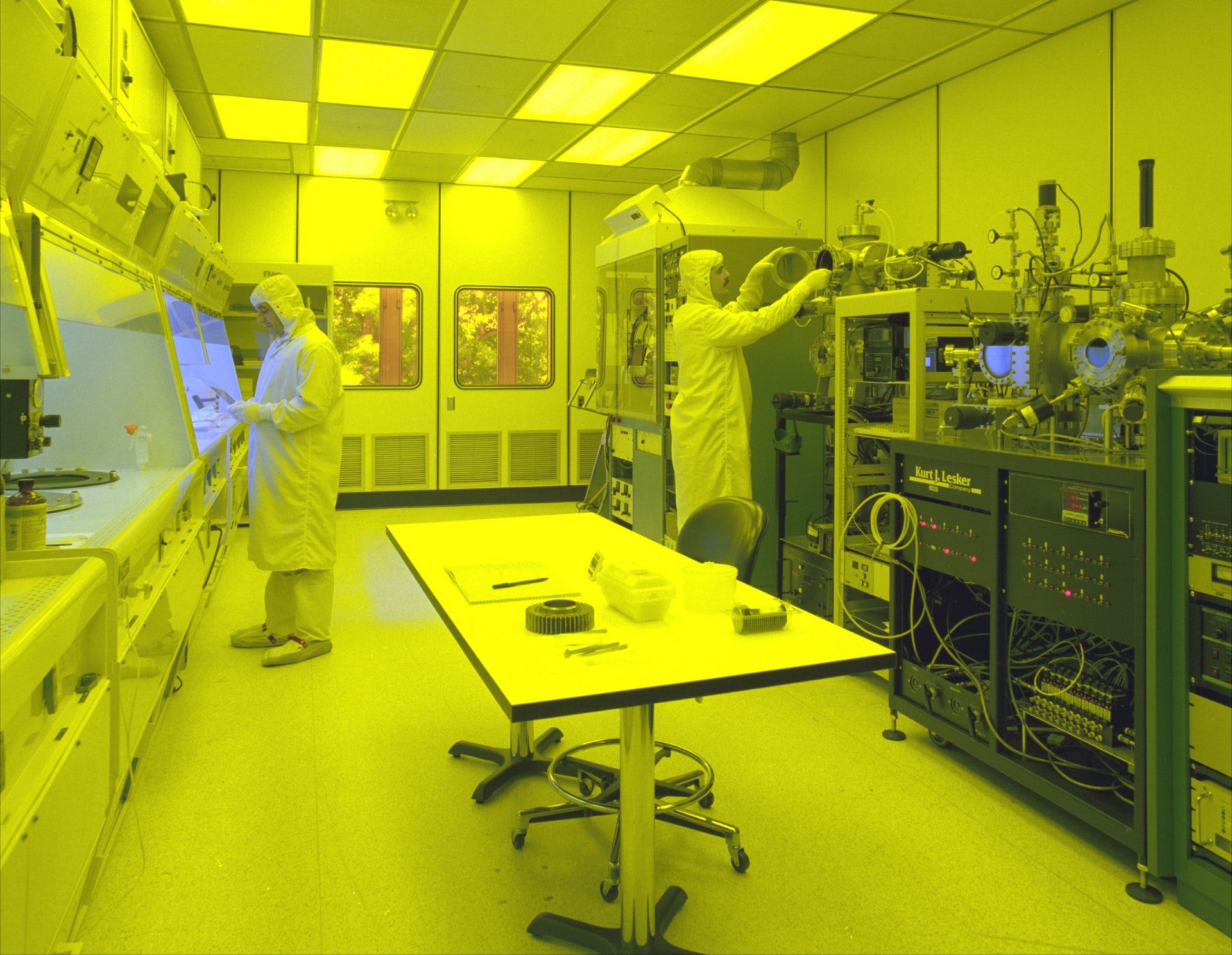
The light used in lithography is typically in the ultraviolet band with a wavelength of 100-400 nanometers — the smaller the wavelength the finer the features that can be drawn onto the photoresist. One of the key reasons behind the ever shrinking size of chips and transistors is the ability to use light of even smaller wavelengths. As of 2022, the Dutch company ASML is the only global supplier of extreme ultraviolet (EUV) lithography systems, which use a wavelength of 13.5nm to produce the world’s smallest and most advanced chips.
The use of UV light is also the reason why clean rooms have a peculiar yellow glow. Normal light sources like bulbs naturally release some UV light which will interfere with and ruin the lithography process. The yellow light comes from sodium-vapour lamps, which produce light with a wavelength of 589 nm, safely larger than anything in the UV spectrum.
Once the chip pattern is printed onto the photoresist, the exposed substrate is shaped by a process called etching. One common technique is plasma etching, where gases are used to remove the upper layers of the substrate that are unprotected by the photoresist. This allows the chip pattern to be transferred to the substrate, creating a 3D pattern on the substrate. Quite often, this pattern is composed of various layers of components which together form the full integrated circuit.
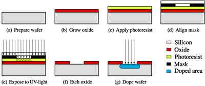
The final step is ionisation, where parts of the exposed substrate that have been etched are bombarded with positive or negatively charged particles to tune the conductivity of different parts of the chip. Ionisation is used, for example, to dope silicon with boron and phosphorus to create p and n type doped silicon.
Once this is done, the chip is packaged and ready to be integrated into whatever device is intended for.
Chip On Your Shoulder
Now that we understand chips better, it’s not so hard to see why they are so important. All modern technology, from smartphones to drones, cannot function without billions of transistors and other semiconductor components. Crucially, chips will also be critical to virtually all future tech. For instance, much of the phenomenal progress in AI relies on devices called graphical processing units, or GPUs, which dramatically speed up computational processes in deep learning. As an example, OpenAI’s GPT-3 language model runs on 10,000 Nvidia V100 GPUs which each have 21 billion transistors. In AI, and other future tech like quantum computing, chip hardware will be just as important as algorithms and software, and governments are becoming increasingly aware of this. This is why the US just recently imposed restrictions blocking Nvidia’s GPU sales to China.
Further complicating the issue is the extremely difficult nature of making chips. Building fabs requires huge amounts of investment to acquire the specialised inputs like cleanrooms and lithography machines. This is why countries that want to ramp up chip production have to cough up billions of dollars.
Today, the state of the art chip manufacturing process is the 5 nm process — the name roughly relates to the size of the components on chip, so the smaller the number the more advanced the process. Currently only Samsung and Taiwan-based TSMC are capable of mass producing 5 nm chips. TSMC plans to make the jump to a 3 nm process, aiming for volume production in the second half of 2022. Nvidia’s H100 GPU — which has 80 billion transistors — is made using TSMC’s 4 nm process, showing the considerable progress towards achieving the 3 nm mark. These improvements in manufacturing processes are the reason for Moore’s Law, which famously states that the number of transistors on a chip roughly doubles every two years.

China, which is going all in on domestic chip production, recently managed to make a 7 nm process chip. This is impressive in its own right, but is also notable considering that China’s state run chip manufacturer, SMIC, was blacklisted by the US government in 2020 which prevented it from buying the advanced EUV lithography machines normally required for these length scales. In response, SMIC managed to make 7 nm chips with older deep ultraviolet (DUV) technology. Although DUV is theoretically capable of making advanced chips, it’s typically used for larger chips in products like cars. But as a result of China’s successes, the US is pushing ASML to stop DUV sales to China as well, causing the company to warn that excessive curbs on business with China could disrupt the broader semiconductor supply chain.
Given their critical nature to modern and future technology, it’s not hard to see why semiconductor chips are called “the new oil”. Semiconductors form the basis for devices like transistors, which in turn are the building blocks for the chips that power everything from today’s phones to tomorrow’s AI models. Now that their importance has reached a mass audience, including even lawmakers in governments, expect the stakes around semiconductors and chips to only get higher.